- 非IC关键词
深圳市中立信电子科技有限公司

- 卖家积分:
 营业执照:已审核经营模式:贸易/代理/分销所在地区:广东 深圳企业网站:
http://www.zlxele.com
收藏本公司 人气:546326
企业档案
- 相关证件:

- 会员类型:
- 会员年限:12年
- 叶先生

- 电话:0755-23956688
- 手机:13410226883
- 王先生
- 电话:0755-23956688
- 阿库IM:
- 地址:深圳市福田区彩田路彩虹新都大厦彩荟阁7A室
- 传真:0755-23956688
- E-mail:sales@zlxele.com

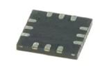
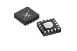
LMK04808BISQE/NOPB Texas Instruments 时钟合成器/抖动清除器
LVCMOS, LVDS, LVPECL
WQFN-64
3.15 V to 3.45 V
250
相关产品


产品信息
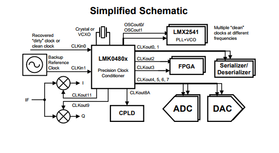
1 Features 3 Description
The LMK0480x family is the industry's highest
1• Ultra-Low RMS Jitter Performance
performance clock conditioner with superior clock
– 111 fs RMS Jitter (12 kHz to 20 MHz) jitter cleaning, generation, and distribution with
– 123 fs RMS Jitter (100 Hz to 20 MHz) advanced features to meet next generation system
• Dual Loop PLLatinum™ PLL Architecture requirements. The dual loop PLLatinum™
architecture is capable of 111 fs rms jitter (12 kHz to
• PLL1 20 MHz) using a low noise VCXO module or sub-200
– Integrated Low-Noise Crystal Oscillator Circuit fs rms jitter (12 kHz to 20 MHz) using a low cost
– Holdover Mode when Input Clocks are Lost external crystal and varactor diode.
– Automatic or Manual Triggering/Recovery The dual loop architecture consists of two high•
PLL2 performance phase-locked loops (PLL), a low-noise
crystal oscillator circuit, and a high-performance
– Normalized PLL Noise Floor of –227 dBc/Hz voltage controlled oscillator (VCO). The first PLL
– Phase Detector Rate up to 155 MHz (PLL1) provides low-noise jitter cleaner functionality
– OSCin Frequency-Doubler while the second PLL (PLL2) performs the clock
generation. PLL1 can be configured to either work
– Integrated Low-Noise VCO with an external VCXO module or the integrated
• 2 Redundant Input Clocks with LOS crystal oscillator with an external tunable crystal and
– Automatic and Manual Switch-Over Modes varactor diode. When paired with a very narrow loop
bandwidth, PLL1 uses the superior close-in phase • 50 % Duty Cycle Output Divides, 1 to 1045 (Even
noise (offsets below 50 kHz) of the VCXO module or and Odd) the tunable crystal to clean the input clock. The
• 12 LVPECL, LVDS, or LVCMOS Programmable output of PLL1 is used as the clean input reference to
Outputs PLL2 where it locks the integrated VCO. The loop
• Digital Delay: Fixed or Dynamically Adjustable bandwidth of PLL2 can be optimized to clean the farout
phase noise (offsets above 50 kHz) where the • 25 ps Step Analog Delay Control.
integrated VCO outperforms the VCXO module or
• 14 Differential Outputs. Up to 26 Single Ended. tunable crystal used in PLL1.
2 Applications
• Data Converter Clocking
• Wireless Infrastructure
• Networking, SONET/SDH, DSLAM
• Medical / Video / Military / Aerospace
• Test and Measurement